Go 750 burnt component ID

Joined
Sep 4, 2012
Messages
3
Location
UK
TomTom Model(s)
go 750 go 820
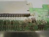
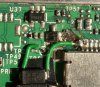
Hi guys, device stopped charging so took a look inside and found a component that connects to the 5v line of the input socket burnt out. Have removed the remains for clarity, if you look at the pic it connects the last pin on the socket to the large-ish (diode ?) to the right, you can see the burn mark between them. Can anybody identify this part for me. The tomtom still works Ok on battery power (charged it up on another tomtom) so would like to repair if possible.
 

Attachments

  • Go-750.jpg
    Go-750.jpg
    26.7 KB · Views: 671
Having a bit of a problem seeing what's happened. Any prayer of reading the component designator from the silkscreen there?

Are all of the traces still intact?
 
Hi, thanks, there are no silk screen marks ajacent to these but there is enough copper to fix to. Had another look with a magnifier and there may be the remains of a small resistor? just below it which is a worry. I guess it needs a member with an open 750 to take a look and advise what they can see.
Update-
on the silk screen this area is surrounded by a box with label TP55,TP54
 
Last edited:
Those would just be "Test Point" indications. No help yet. Yeah, someone with one of the 750's (or a GO 550 would be fine, too) would certainly help. I don't have either of those here.
 
the small bricks with solder on the ends can be resistors, capacitors, fuse or diodes

impossible to tell without removing it and testing, other components connected to it will make a meter read it incorrectly

there should be labels on the board, r = resistor, c = cap d = diode,q = transistor, f = fuse

if a small component fried that bad, most likely its something else connected to it that caused the visable problem

often they have a diode on the power input that shorts the power supply to force its fuse to blow before power goes to anything else if input power is reversed or incorrect
 
there should be labels on the board, r = resistor, c = cap d = diode,q = transistor, f = fuse
...there are no silk screen marks ajacent to these but there is enough copper to fix to.
---
Update-
on the silk screen this area is surrounded by a box with label TP55,TP54
...........
 
Hi, Thanks for your comments so I decided to take another look at it, I'm hoping that someone with electronics experience may be able to hazard a guess as to the likely burnt component.
I've posted a better photo of the board location. I deduced that being a two terminal device wired as is could be an inductor, resistor type, diode type so checked current draw (130ma) across where it should be and connected a small diode(green wired item) to see effect, well this got it working and the battery charges up altho the charging led never goes green so fitting this does seem incorrect.
Anyway this is what info I have-
burnt item was similar in size or slightly larger than resistor 01Y (being a crispy critter difficult to tell)
connected between 5v pin (l/h pin of multi connector in photo) and cathode of MKE diode
Anode of MKE diode goes to Gnd.
resistance of MKE diode --->9.7k or <---O/c
To the right of the top r/h corner of the MKE there looks to be the remains of a small resistor/ l/h end goes to Gnd but other end ? not sure. A picture of a good board would be a godsend.
Any help appreciated.
 

Attachments

  • 750mobo.jpg
    750mobo.jpg
    126.4 KB · Views: 899

Ask a Question

Want to reply to this thread or ask your own question?

You'll need to choose a username for the site, which only take a couple of moments. After that, you can post your question and our members will help you out.

Ask a Question

Members online

No members online now.

Latest resources

Forum statistics

Threads
28,827
Messages
194,368
Members
67,763
Latest member
Gert.Ruland

Latest Threads

Back
Top